witec360 ラマン顕微鏡とHexalight分光器の発売開始
新たなラマンイメージングの基準で、あらゆる方向へ研究を進めましょう


関連: 先進製造技術
二次元材料、量子ドット、ナノワイヤベース材料の成長と特性評価
The growth and manufacture of nanomaterials and nanostructure is fundamentally different to traditional top down manufacturing. Nanowires and 2D materials such as Graphene, MoS2 and hBN are grown by a catalytic self-assembly process and can be used to enhance current devices and build new device architectures. FETs, batteries and filters with unique proporties can now be realised. We provide processes and tools such as our range of ALD and Nanofab CVD, PECVD and ICPCVD tools that enable the controlled growth of nanomaterials.
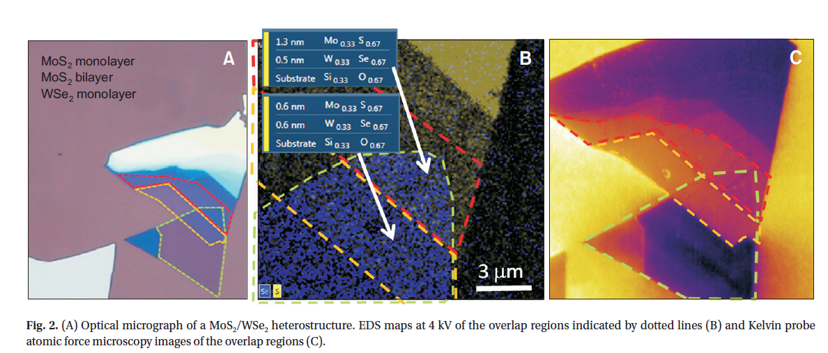
Nanomaterials and the devices based on them can be characterised either by our range of Cypher and MFP-3D AFMs or in the electron microscope using our range of Ultim Max and Ultim Extreme EDS detectors. Many commercial Raman microscopes used in the characterisation of 2D materials use Andor cameras and spectrographs.
© オックスフォード・インストゥルメンツ 2026