witec360 ラマン顕微鏡とHexalight分光器の発売開始
新たなラマンイメージングの基準で、あらゆる方向へ研究を進めましょう


関連: 量子技術
化学から電子輸送まで、3D、2D、1D材料の基本特性の評価
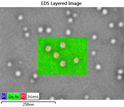
Quantum effects become truly apparent in materials and structures with confined dimensions. Whether that is 2D materials such as graphene or MoS2, InAs quantum dots or III-V nanowires characterising the composition, structure and electronic properties of the materials is key to understanding how they would behave in a manufactured device.
Spectroscopy is the preferred method of analysing 2D materials, ensuring that your graphene is single layer on, not multiple layer, by observing the variation in Raman signal. Our Kymera and Shamrock Spectrographs provide flexible solutions to understanding your materials. At the nanoscale understanding, elemental distribution in materials enables better understanding of the electrical or optical response. Using our latest Ultim Extreme Energy Dispersive X-ray Spectrometer for scanning electron microscopes (SEM) it is possible to characterise elemental distribution in quantum dots down to 10 nm spatial resolution on bulk substrates.
To understand how these material properties affect the electrical properties we have our Optistat range of cryogen-free cryostats with versatile bottom loading, allowing a huge range of sample sizes and structures to be analysed optically and electrically under a wide range of conditions.
© オックスフォード・インストゥルメンツ 2026