

11 January 2013
Oxford Instruments launches LayerProbe - Measure layer thicknesses non-destructively on the SEM
Measures layer thicknesses non-destructively on the SEM
Oxford Instruments NanoAnalysis, a world leader in microanalysis software and systems, has announced the launch of LayerProbeTM, an exciting new software tool for the characterisation of thin layers on a substrate. An option for the Oxford Instruments’ AZtec® EDS microanalysis system, LayerProbe is faster, more cost-effective and higher resolution than dedicated film measurement tools.
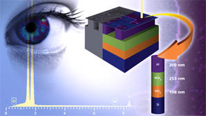
LayerProbe analyses the composition and thickness of the surface and sub-surface layers of a specimen by X-ray microanalysis of the surface alone. Unlike traditional SEM-based thin film measurements based on cross-sectioning of the specimen, LayerProbe analysis is non-destructive. Features only 200 nm wide and layers between 2 nm to 2000 nm thick can be characterised in seconds. LayerProbe is an extension of the AZtec® microanalysis system and can be fitted to most SEMs and FIBs.
According to Dr. Christian Lang, NanoAnalysis Solutions Business Manager, “LayerProbe turns the SEM into a high performance thin film and coating analyser. Comparable non-destructive techniques would require considerable additional investment in dedicated equipment”. Applications include the measurement of thickness and composition of metallisation and dielectric layers in semi-conductors, characterising the active layers in thin film solar cells, industrial coating analysis and an array of nanoscience research areas, such as graphene.
Oxford Instruments NanoAnalysis Managing Director, Dr. Ian Barkshire, stated, “As a business, Oxford Instruments aims to use innovation to turn smart science into world class products that delight our customers. LayerProbe is yet another example of us doing just that".